In-situ power for RF and power electronics
GaN/Si, GaN/SiC and SiC/SiC based devices and related MOCVD processes currently gain increasing interest due to the expected growth rates of the power electronics markets. Recently, at CS ManTech 2015, Yole has forecasted [1]: “2020 exhibits a projected market size for GaN devices of almost $600m (approximately 580,000 x 6” wafers)“ and “SiC device business in 2020 …will exceed $400m”. [Source: Hong Lin of Yole, in Proceedings of CS ManTech 2015] Following this trend, LayTec has further customized its in-situ metrology products for these processes and materials. help our customers to fully exploit the intrinsic advantages offered by wide-bandgap materials (described in Fig. 1) and to manufacture competitive devices with high-yield and cost-efficient processes. 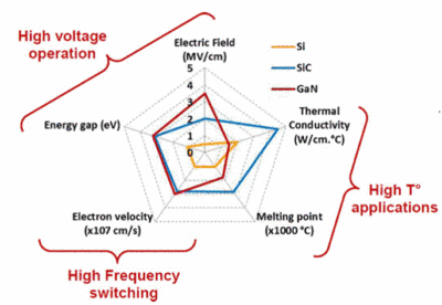
Fig. 1: Summary of Si, SiC and GaN material properties with respect to power electronics applications according to A. Brown, PhD thesis 2015, Glasgow University
Our in-situ metrology systems are powerful tools in your hand: they provide you with real-time information on what is happening in your deposition system. Tight control of process conditions for every layer in every wafer enables you to optimize your growth processes and achieve the best device performance and uniformity. 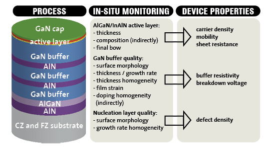
LayTec's in-situ metrology provides the following measurements:
- Reflectance at 3 wavelengths for monitoring of growth rate and morphology (EpiTT and EpiCurve®TT product families)
- Wafer surface temperature (EpiTT and EpiCurve®TT product families)
- Wafer curvature for strain management of layer stacks (EpiCurve®TT)
- Reflectance Anisotropy Spectroscopy (RAS) for III-V surface and interface analysis in the R&D stage (EpiRAS®TT)
You will find a detailed overview of our products for electronic device manufacturing in our Electronics Brochure
Here are some further application examples:
GaN/Si大功率电子设备使用Pyro 400时的准确晶片温度
硅基氮化镓(GaN/Si)设备MOCVD生长过程中的温度测量非常具有挑战性。理论上来说,传统的红外线(IR)高温测量办法可以采用,因为硅衬底在相应生长所需温度范围内完全能够吸收IR。 不过,有种状况会造成反馈控制困难,在工业应用当中也无法实现统计过程的精确控制。 图1所示的就是这种状况:GaN 生长时,温度信号(红色)在±2 K间振荡。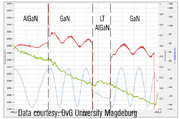
图1:生成压力预应变缓冲层(如曲率数据所述)的GaN/Si模板试验。
红色-温度,
绿色-曲率,
蓝色-反射系数((950nm)
通过与马格德堡大学(Armin Dadgar博士及其团队)和费迪南德-伯恩研究所(Frank Brunner博士)共同研究,我们发现无论IR高温计质量有多好,振荡都是无法避免的。 这种情况是由两种现象之间较为复杂的相互作用造成的:一方面IR透明GaN/AlGaN的应变设计层和缺陷简化了缓冲层的结构,另一方面硅片上的热红外辐射穿过了生长结构。 我们的解决办法就是利用高温测量的波长范围,在该范围内复杂的缓冲层结构Si/AlGaN /GaN/LT-AlGaN/GaN在测量高温时是“隐身”的。
因此,我们选择了LayTec的紫外线(UV)高温计Pyro400,在LED行业中,该仪器几年前已经用在了蓝宝石衬底的GaN生长中。 图2对这些现象进行了演示。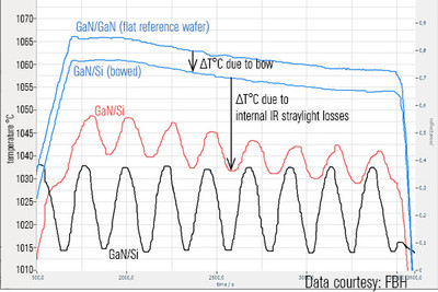
图2:图1模板生长过度,GaN在G3行星式反应器中:
蓝色-UV高温测量
红色-IR高温测量
黑色-反射系数((950 nm)
通过Pyro 400测量的GaN缓冲层温度(下面的蓝色曲线)与Fabry-Perot振荡完全无关。
IR温度(红色)再次显示了振荡,虽然不可避免,但相对于其GaN表面实际温度也下降了-15K!
图1中的晶片转到了FBH(装有两个原位工具:用于UV高温测量的Pyro400和用于IR高温测量的EpiCurve®TT)的反应器(950nm发射系数已校正)、发射系数测量工具和翘曲度测量工具上。 UV高温计(图2-蓝色)显示的晶片温度信号很稳定,GaN生长过程中未发生振荡。同一试验(另述)中参考GaN/GaN晶片的测量结果表明IR高温计和Pyro400均经过了精确校准,在理想平滑GaN/GaN晶片条件下的所示温度完全相同。图2所示的是UV高温测量结果,很明显GaN/Si模板晶片的GaN的实际表面温度为~5K,该结果低于基本平滑的GaN/GaN晶片温度,因为EpiCurve® TT所测硅模板的翘曲度为~100km-1。
另外,很明显IR高温测量信号(红色)中的残留振荡并非最主要。 鉴于热红外辐射与GaN/Si 缓冲层内部结构的相互作用,该温度还会下降约15 (!) K。这种现象是由于通过Si/GaN界面高度缺陷区时硅缓冲层强度下降导致热红外辐射造成的。
这种内部漫射式强度下降现象是由GaN总厚度范围内的Fabry-Perot共振状况决定的,因此也是由IR温度振荡引起的。关于其根本原因方面的详细分析,我们正在编写相关的学术论文,今年晚些时候会出版。我们仅在本通讯稿中对这些结果进行了大致报道,因为其对于大功率电子设备非常重要。 欢迎联系 info@laytec.de.
Expanded nk database and advanced analysis for GaN/SiC-4H HEMTs
RF power transistors like HEMTs based on AlGaN/GaN or InAlN/GaN combine high electron mobility and high critical electric field strength. Their nearly three orders of magnitude lower specific on-resistance (theoretical value) compared to silicon based devices could enable an at least 10-fold reduction of power losses, device size and cost. Typically, the best performance is reached on semi-insulating silicon carbide (SiC). However, the MOCVD growth of the related AlGaN and AlInGaN structures on large SiC-4H wafers needs complex growth recipes for strain management and tight statistical process control (SPC) for high process yields. For this technology, LayTec has expanded its high-temperature nk database and implemented additional real-time analysis routines to feed SPC systems with highly accurate in-situ data. Fig. 1 gives an example:
Fig. 1: AlN buffer growth on SiC-4H in a three-step high-temperature process. The 405 nm reflectance data is highly accurate due to auto-calibration to the true SiC-4H substrate temperature measured in-situ by Pyro 400 (blue - measured, red - fitted reflectance). The fit gives the thickness dAlN=73.2±0.5 nm. Data provided by confidential customer.
The initial AlN growth on SiC-6H is performed at very high wafer temperature (measured by Pyro 400 at ±0.5 K accuracy) and with a sophisticated three-temperature process. This ensures significant defect reduction for the subsequent HEMT growth. Despite the varying wafer temperature in this AlN buffer growth process, the latest real-time analysis function library of LayTec's EpiNet software allows our tools to reach ±0.5 nm accuracy in real-time AlN film thickness measurement. This has been achieved by tightly correlating the absolute SiC-4H wafer temperature with high accuracy SiC-4H and AlN nk optical data and implementing new analysis algorithms that separate reflectance changes caused by temperature ramping from the AlN growth effects.
For further information please ask info@laytec.de.
Mitsubishi Electric Corp. uses in-situ monitoring for crack-free GaN-on-Si HEMTs
The main challenge of GaN based HEMT growth on Si is the lattice mismatch between GaN and AlGaN that causes a high tensile stress and often leads to cracks. Mr. Atsushi Era of Mitsubishi Electric Corporation reported recently about growth of crack-free low-bowing GaN-on-Si HEMTs. [1] To improve the breakdown voltage and power added efficiency, his team grows the GaN buffer layer doped with Fe (GaN:Fe). Mr. Era uses LayTec's EpiCurve® TT to monitor surface roughness, growth rate and wafer bowing.
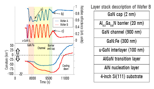
Fig. 1: Left part: In-situ measurements with EpiCurve® TT: Reflectance at 950 nm and curvature data during the growth of Wafers A and B. Right part: Layer stack description of Wafer B.
Fig. 1 shows reflectance and curvature measurements during growth of 2 wafers A (blue) and B (red). The reflectance of Wafer A has a clear slump during the GaN:Fe growth, which indicates a rough surface of GaN:Fe layer. The compressive stress during the GaN growth of wafer A is obviously insufficient to compensate the tensile stress during cooling down. The result is a wafer bow of 40.4 μm in size and a crack over the whole area of Wafer A. The respective AFM (atomic force microscopy) images of surface morphologies (a) and (b) in Fig. 2 confirm this:

Fig 2: AFM images of surface morphologies: (a) - wafer A directly after GaN:Fe growth, (b) - finished wafer A, (c) - finished wafer B. (correlate to a, b, c in Fig. 1)
To suppress 3D island growth in the GaN:Fe, Wafer B is grown with a 100 nm thick undoped GaN interlayer (u-GaN IL) prior to GaN:Fe growth. The reflectance of Wafer B in Fig. 1 shows no slump, which indicates that the GaN:Fe layer grows nicely in 2D mode. The compressive stress is well balanced and the wafer bow is finally suppressed to 15.2 μm, so that Wafer B is nearly flat after down-cooling. Its smooth, crack-free surface is confirmed by AFM in Fig. 2(c). Furthermore, the electron transfer characteristics of a device fabricated on wafer B exhibits ideal pinch-off behavior.
[1] A. Era et al. Growth of crack-free GaN on Si HEMTs with Fe-doped GaN using un-doped GaN interlayer, ICSCRM proceedings (2015)
Examples of HEMT growth before and after optimization
The following example of our industrial customer demonstrates the affect of in-situ monitoring on the final device quality. Real-time in-situ data were used to optimize the growth of high-electron-mobility transistors (HEMTs) on 150 mm Si. Fig. 1 shows in-situ reflectance measured on several points of a wafer (coded in different colors) before growth optimization. It is obvious that the wafer is not homogeneious, which is proved by the X-ray diffraction (XRD) results in Fig. 2.
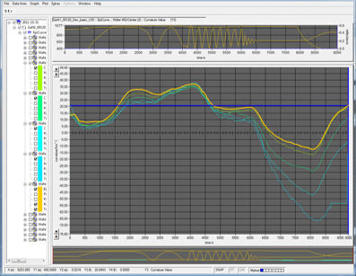
Fig. 1: In-situ reflectance data of non-optimized HEMT growth.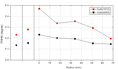
Fig. 2: XRD results of the non-optimized HEMT growth presented in Fig. 1.
LayTec's EpiCurve®TTwas applied for strain engineering, real-time thickness, temperature and homogeneity measurements as well as for Wafer-to-Wafer and Run-to-Run comparison to optimize the growth process. Fig. 3 demonstrate in-situ reflectance measurements of the optimized growth. This data shows a good wafer homogeneity already during the process, which is proved by XRD results in Fig. 4.
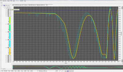
Fig. 3: In-situ reflectance data of optimized HEMT growth
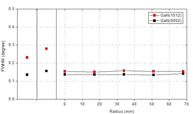
Fig. 4: XRD results of the optimized HEMT growth in Fig. 3.
For further information and more measurement examples please ask info@laytec.de.
In-situ news
- Characterization of 2D materials growth 2022
- Best practices from the field: How to enhance epitaxy process performance by in-situ data
- EpiCurve® TT: AlInN composition control for III-Nitride VCSELs
- Major laser supplier chooses EpiTT FaceT for yield improvement
- EpiTT: optimizing MBE growth of InP-based quantum cascade lasers
- Plenary Talk at EWMOVPE 2019: Metrology for UV-LEDs, VCSEL and Power electronics
- EWMOVPE 2019: In-situ metrology enabling MOCVD on InP based materials on III-V on Si/SiO2 substrates for silicon photonics
- EpiX – a modular wafer mapping station for compound semiconductor research
- EpiTT Band Edge – for MBE of InP based VCSEL devices
- GaAs based edge-emitting high-power IR lasers – yield ramp-up by EpiTT FaceT
- EpiTT VCSEL – shipments to leading VCSEL manufacturer
- In-situ metrology system shipped to GaN-on-SiC customer
- Optimizing quantum cascade laser (QCL) epitaxy with EpiCurve® TTpocket satellite configuration
- In-situ metrology for VCSEL epitaxy with additional spectral reflectance sensing
- UV-C LEDs: AlGaN surface morphology monitored by 280 nm reflectance
- AIXTRON qualifies LayTec EpiNet 2016 software
- IQE equips complete fab with LayTec tools for MOCVD process monitoring
- AbsoluT 400 for temperature calibration of Pyro 400 is on the market!
- In-situ power for RF and power electronics
- Advanced in-situ analysis for UV LEDs

