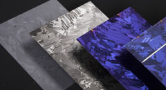
Mono-crystalline silicon (c-Si)-based solar cells

Crystalline silicon cells are manufactured from razor-thin slices of silicon, called wafers, that are either mono-crystalline (c-Si) or multi-crystalline (mc-Si), often known also as poly-crystalline (pc-Si). Recently, quasi mono-crystalline wafers have also expanded the choice of substrate materials available for solar cell manufacturing. ###HIDE### To enable proper function and increase efficiency of solar cells, the manufacturing process comprises several specialized production steps in which LayTec metrology can make considerable contributions.
Improved light trapping is achieved with a wet chemical cell surface texturization process. Additionally, a thinly deposited silicon nitride (SiN) layer forms the anti-reflective coating which gives the cell its typically blue to dark blue or even black appearance. In order to increase its conductivity, the crystal structure is doped. The p-type conductive layer is designed by doping with boron, the n-type by doping with phosphorus. On the front side of the cell, the electrical contact grit bars conduct charge carriers away from a lattice structure of thin conductors, which meet in wide metallic strips called bus bars. On the backside, a large aluminum coating forms the contacting of the cell rear.

LayTec's in-line metrology systems provide sophisticated and highly accurate monitoring of various parameters during mono-crystalline c-Si based solar cell production:
• Wafer thickness measurements
• Texture analysis after etching steps
• Layer thickness and refractive index of passivation layers
• Conductivity measurements of Al back-contact layers
Please contact mail@laytec.de and we will find the best in-line control solution for your individual production line.
###NOHIDE###
Metrology for PV applications
- Flisom chooses LayTec for CIGS quality control
- ILMetro – in-line metrology station for CdTe based thin-film PV
- In-line metrology for ARC coating on structured PV glass
- Mono-crystalline silicon (c-Si)-based solar cells
- Manufacturing of modules: c-Si back end
- CIGS-based solar cells
- CdTe-based solar cells
- Concentrated photovoltaics (CPV)
- Amorphous (a-Si) and microcrystalline (µc-Si) thin film silicon solar cells

