Deflectometry for wafer curvature measurements
The ongoing trend towards bigger wafers in LED and laser production has created new challenges. Wafer bowing, an annoyance with two inch wafers, becomes critical at four inches and above. The curvature creates a differential between the edge and the center of the wafer in its distance to the susceptor. This in turn causes surface temperature deviations across the wafer. The larger the wafer, the greater these temperature deviations.
Problem: Emission wavelength homogeneity
 According to the Solid State Lighting (SSL) road map, an across-wafer wavelength variation of 1 nm is required. This equals a temperature variation of less than 1 K across the wafer. When the wafer bows, the deviation between wafer surface temperature and pocket temperature increases in the case of a 4” sapphire substrate, for example, by up to 20 K or more. This results in a significant indium content variation in the InGaN/GaN multiple quantum wells (MQW) and, as a result, in strong variations in emission wavelength.
Solution: Strain engineering with EpiCurve® TT
 Accurate in-situ monitoring of the wafer curvature helps to minimize bowing-related wafer temperature inhomogeneities, to achieve better photoluminescence (PL) uniformity and, ultimately, leads to higher yields. Find out more on the EpiCurve® TT product page
Asphericity monitoring with advanced resolution
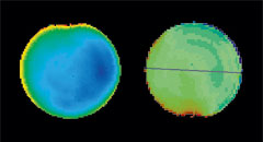
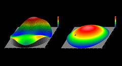
 One of the challenges during buffer growth is the increasing asphericity of the wafer. For processes that potentially cause aspherical wafer curvature, we offer the EpiCurve® TT with the Advanced Resolution (AR) option.
Advantages:
- AR provides information on wafer curvature along two perpendicular directions, radial asphericity and azimuthal asphericity
- AR measures quantity of aspheric component and gives access to information on layer formation
- AR detects relaxation at an early stage and reduces signal fluctuations in the main (spherical) bow measurement caused by aspherical effects
Products that apply this method

