Control and analysis software: Fab integration with EpiNet® and PocketGuard
EpiNet® is a software for control, analysis and optimization of epitaxial processes in production and development of LEDs, laser diodes, VCSEL, HEMT, HBT and other electronic and optoelectronic devices.
The software extracts key figures about wafers’ behavior during growth. In run-to-run control and in statistical process control, these key figures are used to improve yield and process capacity. EpiNet® can be integrated into automated fab workflow providing from simple plain-text files to sophisticated live SECS/GEM integration.
Customer's benefits:
- In-situ process control with ex-situ accuracy even for very thin layers
- Control of complex production processes on operator level
- Fast in-spec / out-of-spec indication for stop or go decisions
- High automation saves operator‘s time, eliminates error sources and makes in-situ control easy without training
- Engineer’s access level for sophisticated data analysis
- High customization

EpiNet provides process-aware algorithms superior to any standard production control system. It can provide process information not available to the growth equipment like complex uniformity information on each wafer. Information which then is intelligently compacted into data that can be handled and analysed by statistical systems. Learn more about Advanced Process Control (APC) with EpiNet.
EpiNet features

Operator's view: PocketGuard
- Quick check of all monitored wafers during the run at one glance
- All wafers are color-coded by user-defined in-spec / out-of-spec criteria and visualized as they are positioned on the susceptor
- In-spec / out-of-spec criteria can be set for all LayTec‘s analysis features
- Customer can easily set up procedures for corrective actions based on PocketGuard information ###NOHIDE###

Wafer-to-Wafer view for post-run analysis
- Analysis results for all wafers shown in separate web charts (polar charts)
- Easy comparison of wafers for run homogeneity check
- Fast detection of outliers – wafer zones that are out of specification limits (red circle) or control limits (yellow circles)

Color plots and line scans
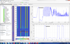
- Color plots (left): time and space-resolved measurements for quick fingerprinting and visualization
- Line scans (low right) show wafer homogeneity during growth
- Time-resolved transients (upper right) are the basis for detailed analysis of growth performance (see Transient view below)###NOHIDE###

Expert analysis: Transient view
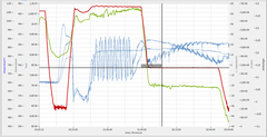
- Complex data comparison of critical process parameters down to single data points across zones, wafers and runs
- Transients can be segmented manually or automatically into growth steps
- Automated analyses of any step to extract process information from raw data (e.g., composition, growth rate etc.)
- Pre-configuration of analyses algorithms as recipes for repeated or automated use###NOHIDE###

Configuration panel: customized run type management
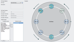
- Visualization of susceptor geometry for setting measurement zones (available for single and multi-pocket configurations)
- Wafer-specific settings for each pocket: susceptor material, pocket material, wafer substrate, thickness and surface condition
For Operators:
- Use of pre-configured analysis recipes
- Automated start of in-situ measurements###NOHIDE###
Product Information
- User-friendly visualization of measured data
- Active real-time GOLDEN RUN analysis
- Toolbox of diagnostic algorithms for all relevant process steps
- Flexible configuration for epi fab-wide SPC (statistical process control) and FDC (fault detection & classification)
- Tight in-house control of your confidential recipes
- Full linescan capability
- Integration into growth system software is possible
- Interactive and recipe-controlled analysis of growth rate, layer thickness and optical constants
- Display of measurements as time-resolved data sets, line scans and color plots
Downloads
- EpiNet Flyer
- EpiNet Data Sheet
- Patterned Sapphire Substrates (PSS): Fast and easy growth analysis with EpiNet

