In-situ solutions for epitaxy: MOVPE, MBE and HVPE
Epitaxy is a technology for growing crystalline thin films on crystalline substrates. Because epitaxy usually has to be controlled at a high level of atomic monolayers, in-situ metrology is indispensable for optimizing material quality and obtaining run-to-run reproducibility in opto-electronic and electronic applications. As a market leader in compound semiconductor epitaxial growth monitoring, LayTec provides in-situ solutions for a variety of epitaxial processes.
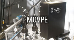
MOVPE is also known as Metalorganic chemical vapor deposition (MOCVD) or Organometallic vapor phase epitaxy (OMVPE). LayTec in-situ metrology systems are available for various MOCVD growth systems such as: ###HIDE###
- Systems with combined main rotation and satellite rotation (reactors of Planetary® type)
- Showerhead-like systems
- Systems with wafer rotation speed of up to 1500 rpm
- R&D type and customized MOCVD growth systems
These products are available for MOCVD process monitoring:
- EpiTT for monitoring wafer temperature, film thickness and surface morphology
- EpiCurve® TT: includes all EpiTT features and additionally monitors wafer thermal stress and defect formation
- EpiRAS® TT: for III-V surface and interface analysis
- EpiR TT: for R&D of new materials and devices, for nanowire growth, VCSEL and laser growth
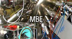
LayTec’s sensors are adaptable to many MBE (Molecular Beam Epitaxy) systems by Riber, Veeco, DCA and VG. Adaptation to other manufacturers’ products and custom-built systems is available on request. The following products are available for MBE process monitoring:###HIDE###
- EpiTT for monitoring wafer temperature, film thickness and surface morphology
- EpiCurve® TT: includes all EpiTT features and additionally monitors wafer thermal stress and defect formation
- EpiRAS® TT: for III-V surface and interface analysis
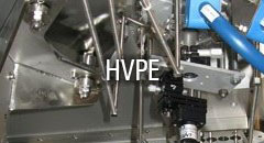
HVPE (Hydride vapor phase epitaxy) is an epitaxial method for the production of compound semiconductor materials that offers a high growth rate and a controlled geometrical size. This technique is used for growing GaN substrates on GaN/sapphire templates. ###HIDE### It is well known that tight growth monitoring is indispensable during HVPE growth. For HVPE applications, LayTec offers:
- EpiTT, which monitors surface roughness, growth rate of the first 10 µm, reflectance and pyrometry at 950 nm. Please learn more about EpiTT for HVPE applications in our Application note
- EpiCurve® TT, which contains all features of EpiTT and monitors additionally the bowing. Find out more about strain engineering for HVPE GaN growth in our Newsletter
Please contact info@laytec.de for further information.
In-situ news
- Characterization of 2D materials growth 2022
- Best practices from the field: How to enhance epitaxy process performance by in-situ data
- EpiCurve® TT: AlInN composition control for III-Nitride VCSELs
- Major laser supplier chooses EpiTT FaceT for yield improvement
- EpiTT: optimizing MBE growth of InP-based quantum cascade lasers
- Plenary Talk at EWMOVPE 2019: Metrology for UV-LEDs, VCSEL and Power electronics
- EWMOVPE 2019: In-situ metrology enabling MOCVD on InP based materials on III-V on Si/SiO2 substrates for silicon photonics
- EpiX – a modular wafer mapping station for compound semiconductor research
- EpiTT Band Edge – for MBE of InP based VCSEL devices
- GaAs based edge-emitting high-power IR lasers – yield ramp-up by EpiTT FaceT
- EpiTT VCSEL – shipments to leading VCSEL manufacturer
- In-situ metrology system shipped to GaN-on-SiC customer
- Optimizing quantum cascade laser (QCL) epitaxy with EpiCurve® TTpocket satellite configuration
- In-situ metrology for VCSEL epitaxy with additional spectral reflectance sensing
- UV-C LEDs: AlGaN surface morphology monitored by 280 nm reflectance
- AIXTRON qualifies LayTec EpiNet 2016 software
- IQE equips complete fab with LayTec tools for MOCVD process monitoring
- AbsoluT 400 for temperature calibration of Pyro 400 is on the market!
- In-situ power for RF and power electronics
- Advanced in-situ analysis for UV LEDs
Links to specific processes