Versatile in-situ metrology for optoelectronics
LayTec is the market leader for in-situ metrology for LED and LASER production systems. In-situ monitoring with LayTec systems during the epitaxial growth process helps identify process defects at the earliest possible stage, enhance yield and improve color uniformity by optimizing processes and enabling optimal control of key parameters.
LayTec in-situ metrology enables fine-tuning of your processes for top performance and tight production line control. The solutions offer absolute wafer temperature readings, accurate wafer bow measurements and precise multiple wavelength reflectance with fully automated analysis. Discover the best standardized metrology system for your individual demands.

VCSELs (vertical-cavity surface-emitting lasers) are currently emerging as a leading technology in rapidly expanding markets like Gesture Recognition, 3D imaging, datacomm and others. For VCSEL epitaxy, LayTec offers in-situ metrology that combines spectral reflectance (for DBR stopbands and cavity dip position sensing) with wafer temperature, growth rate and wafer bow measurements###NOHIDE###. ...more
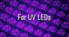
For epitaxial growth of UV LEDs we offer in-situ metrology with significant technology advances: temperature sensing up to 1500°C, AlN buffer layer optimization, high temperature nk database for AlGaN and AlInGaN material classes, monitoring highly doped AlGaN superlattices. ...more

New in-situ results of MIT Lincoln Laboratory (USA) demonstrate optimization of quantum cascade laser (QCL) epitaxy with EpiCurve® TT. Learn more
For growth on infrared (IR) transparent substrates we offer a premium package: direct surface temperature and reflectance monitoring during GaN and SiC growth with Pyro 400
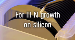
We offer proven metrology for III-N growth on silicon (Si).
Learn more about:
Growth of high quality GaN devices on large-scale Si(111) substrates with EpiCurve® TTEpiCurve® TT
EpiCurve®Triple TT in-situ measurement results of GaN growth on 200 mm diameter Si(111) at IMRE, Singapore: download the newsletter

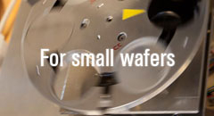
For small wafers, we offer temperature and multiple wavelength reflectance monitoring with products of our EpiTT family
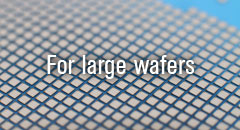
For large wafers when strain becoms a problem, we offer an advanced in-situ solution: Curvature, temperature and reflectance monitoring with LayTec's EpiCurve® TT family of products
In-situ news
- Characterization of 2D materials growth 2022
- Best practices from the field: How to enhance epitaxy process performance by in-situ data
- EpiCurve® TT: AlInN composition control for III-Nitride VCSELs
- Major laser supplier chooses EpiTT FaceT for yield improvement
- EpiTT: optimizing MBE growth of InP-based quantum cascade lasers
- Plenary Talk at EWMOVPE 2019: Metrology for UV-LEDs, VCSEL and Power electronics
- EWMOVPE 2019: In-situ metrology enabling MOCVD on InP based materials on III-V on Si/SiO2 substrates for silicon photonics
- EpiX – a modular wafer mapping station for compound semiconductor research
- EpiTT Band Edge – for MBE of InP based VCSEL devices
- GaAs based edge-emitting high-power IR lasers – yield ramp-up by EpiTT FaceT
- EpiTT VCSEL – shipments to leading VCSEL manufacturer
- In-situ metrology system shipped to GaN-on-SiC customer
- Optimizing quantum cascade laser (QCL) epitaxy with EpiCurve® TTpocket satellite configuration
- In-situ metrology for VCSEL epitaxy with additional spectral reflectance sensing
- UV-C LEDs: AlGaN surface morphology monitored by 280 nm reflectance
- AIXTRON qualifies LayTec EpiNet 2016 software
- IQE equips complete fab with LayTec tools for MOCVD process monitoring
- AbsoluT 400 for temperature calibration of Pyro 400 is on the market!
- In-situ power for RF and power electronics
- Advanced in-situ analysis for UV LEDs