 Epitaxial growth of UV LEDs faces significant challenges: long runs, superlattices, high Al content vs. high doping level, very high growth temperature large wafer bow and many more. LayTec's latest generation of EpiTT and EpiCurve®TT offers significant technology advances to solve most of these problems. Here are some application examples.
In-situ monitoring of high temperature AlN templates for UV LEDs
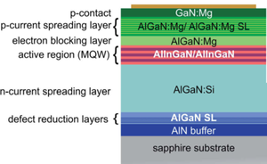
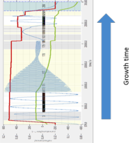
Fig. 1: State-of-the art UV-LED design according to “Chip designs for high efficiency III-nitride based ultraviolet light emitting diodes”, N. L. Ploch, PhD thesis, Technical University of Berlin 2015
Fig. 1 shows a layer stack of a typical UV LED structure to illustrate the growth steps monitored by LayTec's EpiTT and three in-situ parameters: temperature 405 nm reflectance and wafer bow as measured during two MOCVD of a typical UV LED structure. The data demonstrates, how precisely and accurately this combination of in-situ methods monitors the whole process.
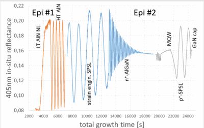
Fig. 2: Two step MOCVD growth of UV-B LED (305 nm): 405 nm in-situ reflectance monitored by EpiTT. (HT=high temperature, LT=low temperature, NL=nucleation layer, SPSL=short-period superlattice)
In the course of LayTec's cooperation with FBH in the consortium "Advanced UV for Life", FBH scientists (Group of Prof. Markus Weyers) have developed a high temperature (HT) MOCVD process for growing low-defect-density AlN/sapphire templates for UV LEDs. The split of the UV LED growth in two separate steps in two different MOCVD systems fully avoids the possible memory effect related interference of AlGaN processes with the growth of high quality AlN buffers. The AlN buffer growth (Fig. 3) was monitored by 3 wavelength reflectance improved for very thick AlN/AlGaN layer stacks and by the emissivity corrected high temperature sensing of EpiTT Gen3. The blue curve is the result of the quantitative analysis of the 3 wavelength reflectance measured by EpiTT Gen3.
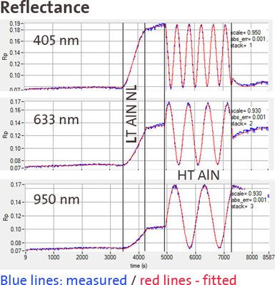
Fig. 3: In-situ reflectance at 405 nm, 633 nm and 950 nm of the two step growth of an AlN template structure for UV LEDs monitored: Blue curves - measured data, red curves - fitted data.
The thickness of the AlN nucleation layer is determined from the fitting curves (red) to be 43.2±0.2 nm, and the AlN high temperature buffer layer thickness to be 524.2±0.5 nm. The consistency of the used high temperature nk database is also obvious from the good agreement of the simulated curve segments in the temperature up-ramping and down-cooling steps.
The key for the unrivaled EpiTT Gen3 high temperature performance is not just the widened temperature sensing range, but, which is more important, also the high temperature nk database (up to 1500°C) for the AlN and AlGaN class of materials and improved performance for double-side polished sapphire wafers.
Alongside with temperature and reflectance, in-situ wafer bow monitoring is a further pathway to process and reactor optimization. Fig. 4 reveals the intrinsic challenge of AlN buffers for UV-LED yield: the wafer bow at the growth temperature of active region (TMQW) is always large, which finally leads to non-uniform UV-LED emission wavelength and, as a result, to lower yields.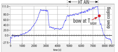
Fig. 4: In-situ wafer bow measurements during growth of UV LED structure.
One of the methods to reduce the strain and annihilate dislocations is a short-period superlattice (SPSL) of GaN/AlN. Internal GaN/AlN interfaces are key for reducing dislocation density. In-situ reflectance at 405 nm in Fig. 5 directly shows the formation of these 160 interfaces between the ~1nm thick GaN/AlN layers. Ex-situ measurements in Fig. 6 confirm this.
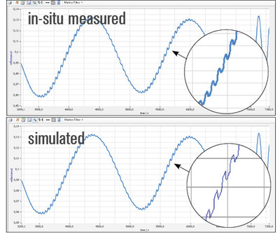
Fig. 5: 405 nm reflectance measured in-situ (above) and simulated (below). The loupe shows the formation of GaN/AlN interfaces of SPSL.
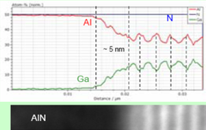
Fig. 6: Ex-situ data: transition from AlN buffer to GaN/AlN superlattice. Red - Al, green - Ga, blue - N.
These examples prove that state-of-the art in-situ metrology is a must for process development and control of such complex devices as UV LEDs. For more information please contact info@laytec.de.
280 nm reflectance senses AlGaN surface morphology
AlGaN buffer layers with high Aluminum content are necessary for optimal UV-C LED performance. But their Band-Edge lies below 300 nm, so the established 405 nm in-situ reflectance is insensitive to the surface morphology of such AlGaN layers. To monitor precisely both AlGaN growth rate and surface morphology during UV-C LED epitaxy, LayTec offers an additional 280 nm reflectance channel that employs a UV-C LED as a light source. Fig. 1 shows the results measured in-situ during the growth of an AlGaN layer: The Fabry-Perot oscillations of the final AlGaN layer are damping out because the band edge of the material shifts toward longer wavelength at the growth temperature. The small reflectance reduction at 12000 s indicates a small roughening of the AlGaN surface.
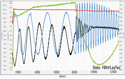
Fig. 1: Growth of AlN/AlGaN(60%Al) on a Sapphire/AlN template in Aixtron CCS 6x2 reactor: black – 280 nm reflectance; blue – 405 nm reflectance; green – high-resolution wafer bow; red – true temperature.
The green line delivers the high-resolution wafer bow data: at ~1000 s the strain changes from compressive towards tensile during AlGaN growth. The wafer bow signal also demonstrates that we have further improved the signal-to-noise ratio of EpiCurve®TT by a full order of magnitude. The green line shows that the wafer curvature noise in this Close Coupled Showerhead® (CCS) reactor is now down to 0.3km-1. With this improvement, in-situ strain balancing or AlGaN lattice constant tuning is now possible with accuracy levels formerly known only for ex-situ XRD methods.
For more information please feel free to contact us at info@laytec.de or call +49 (0)30 89 00 55-0.
This study is supported by Advanced UV for Life funding (grant number 03ZZ0105C, BMBF).
Accurate temperature for pss and double-side polished sapphire in UV LED epitaxy
For UV LEDs, the emitted light usually exits the device structure through the sapphire substrate. Therefore, double-side polished (dsp) sapphire is frequently used. In addition, the front surface of the sapphire substrate can be modified by nano-patterned sapphire substrates (pss) for enhanced light extraction. Both substrate specifics often cause unrecognized artifacts in temperature sensing.
As an example, Fig. 1 shows a temperature step run with three different types of sapphire substrates: dsp, pss and ssp (single side polished).
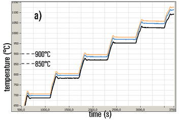
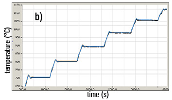
Fig. 1: Temperature step run. True Temperature at 950 nm: blue - pocket W5 (ssp), orange - pocket W6 (dsp), black - pocket W8 (pss)
a) measured by a conventional emissivity corrected IR pyrometer
b) measured by EpiTT Gen3, which eliminates emissivity effects and straylight/defracting effects of the wafer's backside and/or of the pss frontside.
Conventional IR pyrometry (Fig. 1a) measures three different pocket temperatures for these wafer types. While the dsp sapphire substrate at 900°C gives the correct value, ssp is ~10K and pss is ~25K less than dsp. The level of the apparent (but not real) temperature reduction depends on temperature and on the details of back-side roughening, pss patterning and the reactor configuration. EpiTT Gen3, however, comes with new software algorithms that take these specific effects into account and deliver the same accurate pocket temperature for ssp, dsp and pss sapphire substrates (Fig. 1b).
Overcoming the wafer-showerhead gap variation in UV LED epitaxy
For UV LED processes, EpiTT Gen3 can measure temperatures up to 1500°C. However, for accurate temperature sensing another new Gen3 feature is also of importance: two types of metrology heads can now be chosen depending on the specific reactor conditions: the well known fiber-optical heads (FOHs) and the new parallel-beam heads (PBHs). EpiTT with PBHs is the tool of choice e.g. for Close Coupled Showerhead (CCS) reactors, where the wafer-showerhead gap is adjusted to avoid pre-reactions and achieve high growth rates in UV LED processes.
Fig. 1a shows that FOHs suffer from the off-focus situation resulting from such adjustment, while PBHs in Fig. 1b give a very stable reflection and temperature signal under gap variation and, therefore, do not need a rather complex and time-consuming multi-gap calibration.
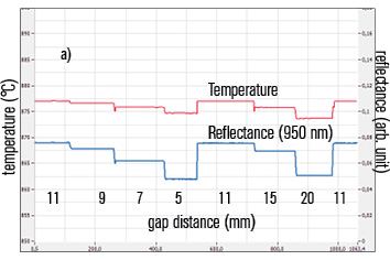
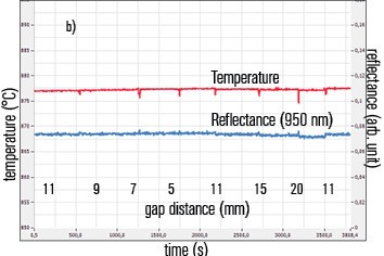
Fig. 1: Reflectance (950 nm) and temperature data during variation of gap size:
a) FOH shows a reflectance drop of ~30% with respective temperature drop of several Kelvins depending on sample structure
b) PBH delivers a stable reflectance and temperature signal. At the standard gap distance (11 mm), both heads measure the same reflectance.
(Data measured with an AbsoluT thermal reference.)
So, for this specific reactor type, Gen3 with parallel beam head (PBH) technology is the best way to achieve accurate temperature measurements using 950 nm reflectance for emissivity correction.
Advanced 405 nm reflectance analysis for AlN buffer optimization in UV LEDs
At our Metrology Workshop during ICNS 2015 in Beijing Prof. Dabing Li of Chinese Academy of Sciencies (CAS) reported about AlN buffer optimization for UV LED growth by means of the 405 nm reflectance. The screenshot in Fig. 1 below shows in-situ reflectance (405 nm) data measured by EpiTT during high temperature MOCVD growth of AlN buffers for UV LEDs. Different surface morphology modes (2D and 3D) show up:
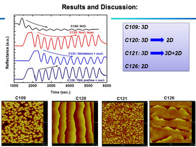
Fig. 1: Transition from 3D island growth to 2D growth in the two-step growth of AlN
You can download the complete talk as a PDF file here
Further reading: X. Sun et.al.: In situ observation of two-step growth of AlN on sapphire using high-temperature metal–organic chemical vapour deposition, CrystEngComm, 2013,15, 6066-6073
In-situ benefits for UV LEDs
- Optimization of UV LED epitaxy
- Early detection of process deviations and wafer defects
- Higher yield
- Better uniformity
- Excellent device performance
Downloads
EMMOVPE 2019: 280 nm reflectometry – helpful tool for in-situ control of AlN-based MOVPE-growthApplication Note: In-situ metrology solutions for UV LED growth
In-situ news
- Characterization of 2D materials growth 2022
- Best practices from the field: How to enhance epitaxy process performance by in-situ data
- EpiCurve® TT: AlInN composition control for III-Nitride VCSELs
- Major laser supplier chooses EpiTT FaceT for yield improvement
- EpiTT: optimizing MBE growth of InP-based quantum cascade lasers
- Plenary Talk at EWMOVPE 2019: Metrology for UV-LEDs, VCSEL and Power electronics
- EWMOVPE 2019: In-situ metrology enabling MOCVD on InP based materials on III-V on Si/SiO2 substrates for silicon photonics
- EpiX – a modular wafer mapping station for compound semiconductor research
- EpiTT Band Edge – for MBE of InP based VCSEL devices
- GaAs based edge-emitting high-power IR lasers – yield ramp-up by EpiTT FaceT
- EpiTT VCSEL – shipments to leading VCSEL manufacturer
- In-situ metrology system shipped to GaN-on-SiC customer
- Optimizing quantum cascade laser (QCL) epitaxy with EpiCurve® TTpocket satellite configuration
- In-situ metrology for VCSEL epitaxy with additional spectral reflectance sensing
- UV-C LEDs: AlGaN surface morphology monitored by 280 nm reflectance
- AIXTRON qualifies LayTec EpiNet 2016 software
- IQE equips complete fab with LayTec tools for MOCVD process monitoring
- AbsoluT 400 for temperature calibration of Pyro 400 is on the market!
- In-situ power for RF and power electronics
- Advanced in-situ analysis for UV LEDs
Advanced UV for Life
LayTec is a partner of the consortium "Advanced UV for Life" funded by the German Federal Ministry of Education and Research within the program "Twenty20 - Partnership for Innovation" (grant number 03ZZ0105C).
