EpiTT in GaAs wafer foundry: fast recalibration of GaAs/AlGaAs MOCVD
Operating MOCVD in III-V foundry businesses faces the specific challenge of frequent change of growth recipes for different customers with specific MOCVD re-calibration needs. In cooperation with the National Research Council of Canada and JENOPTIK (Germany), LayTec has developed a method for a fast and high-accuracy in-situ calibration of AlGaAs composition and AlGaAs growth rate.
In-situ reflectance based AlGaAs process calibration GaAs wafer temperature sensing by our in-situ tool EpiTT (calibrated by AbsoluT) can fully replace established but time-consuming ex-situ calibrations (XRD, PL and others). Thereby, this new approach shortens significantly the non-productive re-calibration time between MOCVD runs for different customers.

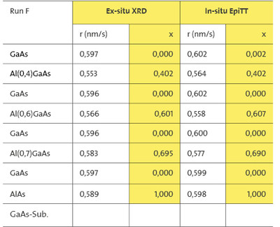
Table 1: In a multiple 450 nm AlGaAs layer stack (sandwiched between 750 nm GaAs layers) the in-situ measured AlGaAs composition x and growth rate r exactly matches the XRD reference measurement. A new, highly accurate AlGaAs refractive index database in the 600°C-710°C temperature range and precise wafer temperature measurement with AbsoluT calibration have been applied.
Analysis of nanometer scaled quaternary films with EpiNet 2016
LayTec's new release of the control and analysis software EpiNet 2016 offers completely new analysis features for our customers interested in high-accuracy statistical process control (SPC) of related device growth processes. Fig. 1 gives an example:

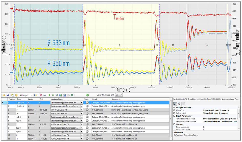
Fig. 1: Screenshot of the EpiNet 2016: data analysis of an InGaAsP/InP device structure on InP(001): the thickness of the three very thin InGaAsP layers in steps 2, 6, 10 is: 28.5 nm, 48.7 nm and 100.3 nm respectively. The table in the lower part of the figure gives the sequence of analysis functions for routine and automated SPC of this device growth process.
The thickness of very thin InGaAsP layers in a device stack grown in an AIXTRON Planetary Reactor® on InP(001) is determined by a well selected set of automated analysis operations. First, several InP layers are utilized for permanent in-situ high-accuracy re-calibration of all reflectance channels (yellow lines) in long lasting epi runs. Second, the lattice matching of the quaternary layers is verified by wafer bow analysis (not shown). Third, the composition of the quaternary material is determined at the thick InGaAsP layer in step #14. And finally, based on this information, the thickness of the thin InGaAsP layers in steps #2, #6 and #10 is accurately measured by double-wavelength thickness analysis.
For better understanding of growth processes, LayTec offers related training courses for process engineers and quality managers. To learn more, please contact info@laytec.de or call our sales engineer +49 30 89 00 55-0.
Products for SEMI materials
- III-N, III-As, P: EpiTT, EpiCurve®TT
- GaN/Sapphire, SiC: Pyro 400
- Cubic III-V, IV: EpiRAS®
In-situ news
- Characterization of 2D materials growth 2022
- Best practices from the field: How to enhance epitaxy process performance by in-situ data
- EpiCurve® TT: AlInN composition control for III-Nitride VCSELs
- Major laser supplier chooses EpiTT FaceT for yield improvement
- EpiTT: optimizing MBE growth of InP-based quantum cascade lasers
- Plenary Talk at EWMOVPE 2019: Metrology for UV-LEDs, VCSEL and Power electronics
- EWMOVPE 2019: In-situ metrology enabling MOCVD on InP based materials on III-V on Si/SiO2 substrates for silicon photonics
- EpiX – a modular wafer mapping station for compound semiconductor research
- EpiTT Band Edge – for MBE of InP based VCSEL devices
- GaAs based edge-emitting high-power IR lasers – yield ramp-up by EpiTT FaceT
- EpiTT VCSEL – shipments to leading VCSEL manufacturer
- In-situ metrology system shipped to GaN-on-SiC customer
- Optimizing quantum cascade laser (QCL) epitaxy with EpiCurve® TTpocket satellite configuration
- In-situ metrology for VCSEL epitaxy with additional spectral reflectance sensing
- UV-C LEDs: AlGaN surface morphology monitored by 280 nm reflectance
- AIXTRON qualifies LayTec EpiNet 2016 software
- IQE equips complete fab with LayTec tools for MOCVD process monitoring
- AbsoluT 400 for temperature calibration of Pyro 400 is on the market!
- In-situ power for RF and power electronics
- Advanced in-situ analysis for UV LEDs

