CIGS-based solar cells

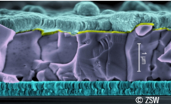
Cu(In,Ga)Se2 (CIGS) is currently the most successful thin-film photovoltaic technology because of its high efficiency potential. However, the quaternary CIGS absorber has to be controlled tightly to reproduce the high efficiencies created in labs on a production scale. The typical layer stack is comprised of molybdenum, CIGS, a buffer (e.g. CdS), i-ZnO and a transparent conducting oxide (TCO) on top. ###NOHIDE### The layers are deposited by sputtering, co-evaporation, and chemical bath deposition. Because each layer dramatically influences the quality of the final device, all five layers must be grown within narrow target specs.

For CIGS applications, LayTec‘s metrology systems can be seamlessly integrated into production lines on a 24/7 basis. Our Flames measures reflectance and film thickness on all layers. The in-line photoluminescence system PearL determines the bandgap of the CIGS absorber and monitors derviations in the composition of CIGS with high sensititivity. The eddy-current sensor EddY measures conductivity of all conducting layers. ###NOHIDE###

LayTec‘s spectroscopic photoluminescence (PL) system PearL is an ideal tool for in-line CIGS monitoring in high-volume solar cell production. It has numerous advantages under production conditions:
- reliable CIGS characterization across the full module length at different points;
- spatially resolved information about band gap, material composition and quality of the CIGS absorber material;
- analysis of the absorber parameters directly after its deposition without interference of other layers;
- fast identification of faulty substrates before the cost-intensive back-end processing;
- fast measurement time of only 0.1 s###NOHIDE###
Please learn more on the PearL site or in our PDF newsletter
Metrology for PV applications
- Flisom chooses LayTec for CIGS quality control
- ILMetro – in-line metrology station for CdTe based thin-film PV
- In-line metrology for ARC coating on structured PV glass
- Mono-crystalline silicon (c-Si)-based solar cells
- Manufacturing of modules: c-Si back end
- CIGS-based solar cells
- CdTe-based solar cells
- Concentrated photovoltaics (CPV)
- Amorphous (a-Si) and microcrystalline (µc-Si) thin film silicon solar cells

