LayTec’s metrology tools are of critical importance in the R&D labs of research organizations where new thin-film materials, processes and device structures are developed. Our strength lies in understanding the demands of our customers and modifying and combining existing products into new systems that can be applied to an extremely wide range of R&D applications.
LayTec`s invited talk at ICCGE-19 / OMVPE-19
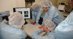
Dr. Kolja Haberland of LayTec gave an invited talk about "State-of-the-art in-situ metrology during OMVPE in academic research and industry" at ICCGE-19 / OMVPE-19 in Keystone, Colorado, USA.
Please find more detaills in thefollowing presentation.
LayTec metrology speeds up process development on 100 mm (11-22) GaN / r-PSS
Dr. Frank Brunner of FBH Berlin, Germany presented his latest results on growth of (11-22) GaN / r-PSS in an AIX 2600G3-HT reactor (8x4” config¬uration) at last week’s OMVPE Workshop in BigSky (Montana). Please find more details about "Large area heteroepitaxial (11-22) - GaN growth" in the following presentation.
In-situ photoluminescence of growing III-Nitride LED structures
In a collaboration between LayTec and Prof. Dirk Rueter´s group at University of Applied Sciences Ruhr West a break-through has been achieved regarding the real-time monitoring of InGaN/GaN quantum well emission wavelength during MOCVD growth. It is well known that room temperature wafer based photoluminescence (PL) measurements provide an excellent forecast of the emission wavelength and emission intensity of the later LED devices. This prototype in-situ PL system in [1] team workes at growth temperatures with LayTec Pyro 400 in a commercial multi-wafer MOCVD reactor. The related paper [1] was rocketed immediately to the status of “most downloaded Journal of Crystal Growth articles” from Science Direct. This work is supported under grant KF3242801NT3 by BMWi (German Federal Government).
[1] C. Prall et al. in Journal of Crystal Growth 415 (2015), 1–6.

Fig.1: In-situ spectra of growing InGaN MQW structure (solid lines) at wafer temperature of 690 °C. The InGaN PL peak wavelength was extracted from Gaussian fits (dashed lines) to eliminate the FPOs.
In-situ metrology for graphene growth
For several years, graphene has been the subject of intense research activity aimed at exploiting its unique properties. Unbreakable and foldable touch screens for mobile phones, faster computer chips, batteries of higher capacity – these are just a few of graphene’s applications. Although the growth of graphene is a very new and complex process, we have developed a solution for in-situ reflectance analysis of the surface changes during the growth.
The first tests have been conducted during graphene growth on copper/silicon (Cu/Si) in a commercial CVD reactor. Our in-situ reflectometer has clearly demonstrated its sensitivity to surface processes like de-oxidation and roughening during graphene CVD on Cu. Furthermore, we could see that in case of growth on Cu/Si, the combination of temperature, low pressure and CH4 supply does change the surface properties of the copper substrate and causes copper removal from the surface. Therefore, a sensor able to monitor in-situ both surface temperature and reflectance, like LayTec’s EpiTT, can deliver valuable information to understand and optimize the deposition process.
Further systematic in-situ studies by our academic customers will give new insights into the physics and chemistry of such processes, and complement the results of other, more complicated techniques as spectroscopic ellipsometry. For future large-scale production reactors, where ellipsometry ports usually cannot be easily integrated, either normal incidence 3-wavelength reflectance (EpiTT) or even UV/visible spectroscopic reflectance (EpiR DA TT) could serve as efficient in-situ metrology tools both for R&D and future process control.
For details of the study and the first tentative results please ask info@laytec.de for our Graphene Application Note.
Solutions that fit your needs
If you’re considering using LayTec tools on new materials, in a different deposition environment or even ex-situ on a test bench, don’t hesitate to get in touch. Our flexible and modular product concept allows us to quickly develop a solution to fit your needs.
We are open to working in close collaboration with research customers and universities, with industry customers in joint-development projects (JDPs) and with equipment vendors in OEM projects. Our highly qualified engineers in the R&D Department and the Department of Application Engineering will be pleased to answer your phone call or email:
+49 (0)30 89 00 55-0 / info@laytec.de.
Public funded project
NextLED - Next generation LED technology for LED with 235 lm / W
Partner: Aixtron SE, Herzogenrath/Germany; Rheinisch-Westfälische Technische Hochschule Aachen (RWTH Aachen), Germany

Grant number 13N14224.(BMBF)
UV Power - In-situ control of epitaxy and plasma processes for UV-LED manufacturing
Partner: Osram Opto Semiconductors GmbH, Germany; Ferdinand-Braun-Institut (FBH) Germany; TU Berlin, Germany; UVphotonics NT GmbH, Germany
Grant number 03ZZ0134D.(BMBF)
GIMMIK - Graph processing on 200mm wafers for microelectronic applications
Partner: Aixtron SE, Herzogenrath/Germany; Infineon Technologies AG, Munich/Germany; Protemics GmbH, Aachen/Germany; IHP GmbH – Innovations for High Performance Microelectronics/Leibniz-Institut für innovative Mikroelektronik, Frankfurt(Oder)/Germany; Rheinisch-Westfälische Technische Hochschule Aachen (RWTH Aachen) Aachen/Germany.
Grant number 03XP0210B.(BMBF)
MOCVD 4.2 - Optimized manufacturing of compound semiconductors for enhanced impacts in the energy supply
Partner: Aixtron SE, Herzogenrath/Germany; Institut für Mikroelektronik Stuttgart, Stuttgart/Germany; Rheinisch-Westfälische Technische Hochschule Aachen (RWTH Aachen) Aachen/Germany; Azur Space Solar Power GmbH, Heilbronn/Germany.
Grant number 0324237B (BMWI)
SmartLine – Smart in-line metrology and control for boosting the yield and quality of high-volume manufacturing of organic electronics
Partner: Aristotelio Panepistimio Thessalonikis, Thessaloniki/Greece; Centro Ricerche Fiat SCPA, Orbassano/Italy; Aixtron SE, Herzogenrath/Germany; Suragus GmbH, Dresden/Germany; IBS Precision Engineering BV, Eindhoven/Netherlands; Organic Electronic Technologies Private Company IKE, Thessaloniki/Greece
![]()
Grant number 768707