Patterned Sapphire Substrates (PSS): Fast and easy growth analysis
Patterned Sapphire Substrates (PSS) are becoming indispensable in GaN LED production. LEDs grown on PSS typically have larger light output and better crystal quality. To take MOCVD processes on PSS under tight in-situ control, some additional efforts are needed. Every kind of patterned substrate, e.g. cone, dome or spherical pattern, requires individual in-situ calibration of the reflectance signal just before the process.
LayTec‘s in-situ metrology software EpiNet can be individually customized for patterned substrates. Our users can expand the substrate database of the software by themselves. LayTec‘s Calibration Manual explains how to measure PSS reflectance in different pockets in one single calibration run. If required, LayTec also offers related customer trainings. Once the initial reflectance values of the PSS substrates are uploaded to the EpiNet substrate database, the operator has the option to choose the needed substrate type in the RunType‘s Material Spec window as shown in Fig. 1. As a result, all PSS wafers can be monitored with the same accuracy as standard sapphire substrates.
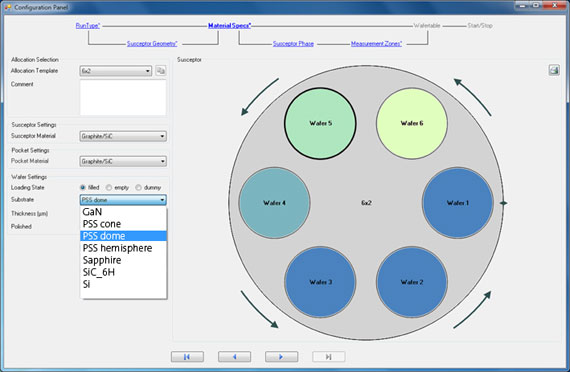
Fig. 1: RunType’s Material Spec window of EpiNet software with customized database extended with additional PSS types.
Fig. 2 demonstrates a reflectance signal during GaN growth on PSS. The initial reflectance of the bare PSS substrates is typically lower than that of standard single-polished sapphire. In addition, the inital reflectance of the three wavelengths (405 / 633 / 950 nm) is very different because the interaction of light with the 3 dimensional nano-/micro-patterning (scattering, diffraction, interference) strongly depends on the wavelength. In the screenshot (Fig. 2), the increasing reflectance amplitude (after ~4000 s of the growth process) shows the coalescence process of GaN. After ~8050 s, the 405 nm reflectance stays stable at 15.5%, which is an indication of the GaN surface quality improvement. The 633 nm and 950 nm reflectance signals have well developed interference patterns.
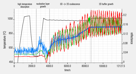
Fig. 2: GaN growth on PSS measured by EpiCurve® TT installed on AIXTRON PLanetary® G3 reactor at FBH, Berlin, Germany. Screenshot of EpiNet software: reflectance at 405 nm (blue), 633 nm (green), 950 nm (red); True Temperature (black).
Interestingly, some lateral non-uniformity of the PSS structures across the wafer obviously show up in these data. The initial 405 nm reflectance on the bare PSS substrate (0... ~4000 s) is noisy, while 633 nm and 950 nm reflectance is rather smooth. The 405 nm wavelength is in resonance with some geometric parameters of the pattern‘s structure, which is non-uniform. As soon as the GaN buffer is thick enough, the 405 nm light does not reach the pattern anymore because of the absorption in the GaN. Hence, the 405 nm reflectance „noise“ reduces because the GaN surface is rather smooth. However, the interference patterns of the 633/950 nm reflectance look „noisy“ during 2 D buffer growth. Obviously, the initial non-uniformity of the PSS structure causes a certain non-uniformity in the GaN thickness.
LayTec‘s EpiNet software makes it easy to take LED growth processes on PSS under tight in-situ control. It quickly identifies even quality deviations and non-uniformities of the PSS substrates. Furthermore, the software also contains fitting of thin layers, wafer bow calculation and many further features indispensable for growth on PSS.
For further information please ask for EpiNet Flyer or contact: sales@laytec.de.
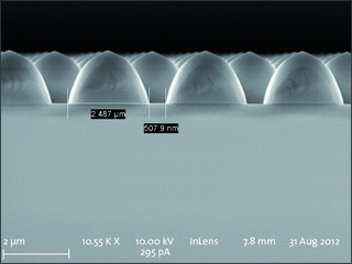
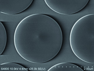
PSS REM images: domes and cones
In-situ news
- Characterization of 2D materials growth 2022
- Best practices from the field: How to enhance epitaxy process performance by in-situ data
- EpiCurve® TT: AlInN composition control for III-Nitride VCSELs
- Major laser supplier chooses EpiTT FaceT for yield improvement
- EpiTT: optimizing MBE growth of InP-based quantum cascade lasers
- Plenary Talk at EWMOVPE 2019: Metrology for UV-LEDs, VCSEL and Power electronics
- EWMOVPE 2019: In-situ metrology enabling MOCVD on InP based materials on III-V on Si/SiO2 substrates for silicon photonics
- EpiX – a modular wafer mapping station for compound semiconductor research
- EpiTT Band Edge – for MBE of InP based VCSEL devices
- GaAs based edge-emitting high-power IR lasers – yield ramp-up by EpiTT FaceT
- EpiTT VCSEL – shipments to leading VCSEL manufacturer
- In-situ metrology system shipped to GaN-on-SiC customer
- Optimizing quantum cascade laser (QCL) epitaxy with EpiCurve® TTpocket satellite configuration
- In-situ metrology for VCSEL epitaxy with additional spectral reflectance sensing
- UV-C LEDs: AlGaN surface morphology monitored by 280 nm reflectance
- AIXTRON qualifies LayTec EpiNet 2016 software
- IQE equips complete fab with LayTec tools for MOCVD process monitoring
- AbsoluT 400 for temperature calibration of Pyro 400 is on the market!
- In-situ power for RF and power electronics
- Advanced in-situ analysis for UV LEDs