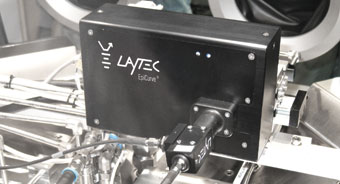
 為了克服大尺寸晶圓(4 吋、6 吋或 8 吋)的挑戰,您需要先進的 EpiCurve® TT 系統。EpiCurve® TT 結合晶圓曲率量測和所有 EpiTT 的功能:發射率校正測溫和三種波常反射率成長速度/厚度量測。此工具能助您避免破裂,讓晶圓平整,並控制溫度均勻性。各種曲率工具皆可搭配先進解析度(Advanced Resolution,AR)曲率量測工具控制晶圓弓形度的飛球面性(EpiCurve® TT AR)。
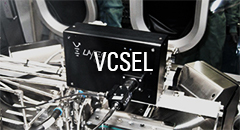
LayTec has customized and expanded EpiCurve®TT's performance for VCSEL epitaxy: an additional measurement head for spectral reflectance sensing can be mounted on a conventional EpiCurve®TT system. This allows integrating the full EpiCurve®TT performance with the spectral monitoring of DBR stop-bands and cavity dip position. ...more
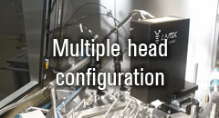
LayTec 提供 EpiCurve® TT 與 EpiTT產品系列的搭配:EpiCurve®Twin TT 共有兩個 EpiTT 頭,EpiCurve®Triple TT 有三個 EpiTT 光學頭,可在獨立位置測量溫度和反射率。
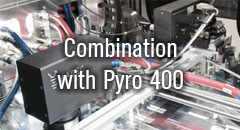
對於弓形紅外線透明基板如藍寶石或碳化矽,傳統紅外線高溫計只能量測到載體溫度。LayTec Pyro 400 直接測量藍寶石和碳化矽中氮化鎵表面溫度,以直接控制氮化銦鎵多量子井層的成長。Pyro 400 搭配 EpiCurve® TT 提供您所有即時成長參數,並以藍光、綠 LED 和雷射二極體監控量子井成長。 ... 更多 ... more
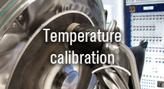
對於包含 EpiCurve 光學頭的系統,Laytec 提供獨特的溫度校準工具 AbsoluT。AbsoluT為小型手持裝置,將相同的絕對溫度參考點設定在各 EpiTT 、不同晶圓環、不同反應器和不同批次進行測量,達到精準的環對環、反應器對反應器和批次間的溫度校準。 ... 更多 ...more
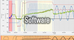
所有 LayTec 即時系統皆具備 LayTec 專門為製程最佳化、分析和控制所開發的軟體。我們的軟體解決方案可以在 MOCVD 晶圓廠控制多個系統,同時監控所有批次運行,並在依據先進製程控制(Advanced Process Control,APC)支援作業員決定”停線與否”。 ... 更多 ... more
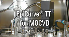
EpiCurve® TT 系列的所有產品皆適用所有 MOCVD 成長系統,如具備衛星旋轉製程的系統、類面沉積製程、研發型和客製 MOCVD 成長系統等。請下載 EpiCurve® TT 規格書深入瞭解
Detecting thin-film strain in-situ during epi growth through the tiny openings of the showerhead view-ports is a challenge. However, with our advanced software algorithms, in-situ strain balancing or AlGaN lattice constant tuning is now possible with accuracy levels formerly known only for ex-situ XRD methods. ...more
LayTec 的感測器可相容於 Riber、Veeco、DCA 和 VG 的 MBE 系統。用於其他製造商產品和客製系統,可視需求提供。請下載我們的應用須知深入瞭解:適用於 MBE 的 EpiCurve® TT
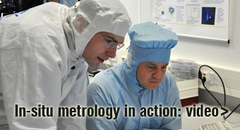
To see LayTec in-situ metrology live, you can watch a video that we have taken at a customer site. In a short lab tour at FBH Berlin in Germany you will see how EpiCurve® TT and EpiRAS TT monitor LED and laser growth and help optimize the processes. ... more
Product information
Fields of application
- GaN LED and laser diode production
- III-Nitride growth on silicon
- GaAs/AlGaInP/InP laser diode production
- Triple-junction solar cell production on GaAs, Ge, Si
- SiC for power electronics
- R&D for new materials and devices
Product Features
- Wafer-selective curvature measurements in the curvature range from -7000 km-1 (convex) to +800 km-1 (concave)
- Versions with a blue laser provide measurements on double-sided polished and patterned substrates
- Aspherical bowing curvature measurements with an Advanced Resolution (AR) option
Emissivity Corrected Pyrometry:
- Temperature range: T = 450°C to 1300°C for large viewport systems / T = 500°C to 1400°C for narrow viewport systems / other temperature ranges on request, e.g. 1500°C for UV LED applications, 1700°C for SiC
- Accuracy better than 1 K
- Wafer and area selective measurements
- True wafer temperature for opaque semiconductors such as InP, Graphite (SbS)
- Pocket temperature for GaN, Sapphire and SiC
Reflectance at three wavelengths:
- 950 nm, 633 nm and 405 nm
- growth rate, layer thickness, roughness and other layer qualities
Downloads
- Application Note: In-situ monitoring of 2D materials
- EpiCurve® TT Data Sheet
- Product Discontinuation Notification
- Brochure: In-situ metrology for LED and laser production
- Brochure: In-situ solutions for process optimization in electronic device manufacturing
- Application Note: In-situ metrology for concentrated solar cells
- Application Note: EpiCurve® TT for MBE
- Presentation: In-situ characterization of 2D materials growth
- Presentation: ICP Etching Process Improvement by in-situ metrology
In-situ product portfolio