Strain engineering for GaAs-based laser structures
It is known that MOVPE growth of AlGaAs on GaAs is limited by lattice mismatch at room temperature and not at growth temperature [1]. The resulting wafer bow may cause problems during the subsequent processing and chip mounting of edge-emitting laser diodes.
In order to reduce the wafer bow at room temperature, Dr. Andre Maaßdorf and his team at FBH Berlin (Germany) have developed a special scheme for strain engineering: they add phosphorus (P) and replace Al0.85GaAs by Al0.85GaAs0.96P in a distributed manner.
To control their laser growth in an Aixtron MOCVD system in real-time, the team uses LayTec’s EpiCurve® TT for simultaneous curvature, pyrometry and reflectance measurements to observe the curvature development, the temperature and the layer thickness.

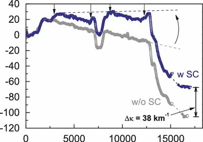
Fig.1: In-situ curvature data of laser structure with (blue) and without (grey) SC layers (marked by arrows). Dashed lines show the envelopes of the curvature in both cases. [1]
Fig. 1 shows two curvature transients of an edge-emitting laser structure with and without strain-compensating (SC) AlGaAsP layers indicated by vertical arrows. These layers directly replace AlGaAs and have a thickness in the range of 230–350 nm.
The dashed lines show the curvature envelopes of both transients. The envelope for the non-compensated structure is tilted (grey dashed line), which leads to an increased convex bow throughout growth, but the envelope of the compensated structure is flat (blue dashed line).
Furthermore, we can see that compressive strain occurring during cool down (after ~1250 s) remains the same in both cases as it is caused by different thermal expansion of layer and substrate. However, the final room temperature curvature of the compensated structure is reduced by 38 km-1 (Fig. 1).
Finally, Dr. Maaßdorf also describes the procedure for measuring the thermal expansion coefficient of ternary compound materials by EpiCurve® TT [2]. LayTec is looking forward to further results and further exciting in-situ measurement data!
For further information please contact info@laytec.de.
[1] A. Maassdorf et.al., J. Cryst. Growth 370 (2013) 150-153
[2] A. Maaßdorf et al., J. Appl. Phys. 114, 033501 (2013)
In-situ news
- Characterization of 2D materials growth 2022
- Best practices from the field: How to enhance epitaxy process performance by in-situ data
- EpiCurve® TT: AlInN composition control for III-Nitride VCSELs
- Major laser supplier chooses EpiTT FaceT for yield improvement
- EpiTT: optimizing MBE growth of InP-based quantum cascade lasers
- Plenary Talk at EWMOVPE 2019: Metrology for UV-LEDs, VCSEL and Power electronics
- EWMOVPE 2019: In-situ metrology enabling MOCVD on InP based materials on III-V on Si/SiO2 substrates for silicon photonics
- EpiX – a modular wafer mapping station for compound semiconductor research
- EpiTT Band Edge – for MBE of InP based VCSEL devices
- GaAs based edge-emitting high-power IR lasers – yield ramp-up by EpiTT FaceT
- EpiTT VCSEL – shipments to leading VCSEL manufacturer
- In-situ metrology system shipped to GaN-on-SiC customer
- Optimizing quantum cascade laser (QCL) epitaxy with EpiCurve® TTpocket satellite configuration
- In-situ metrology for VCSEL epitaxy with additional spectral reflectance sensing
- UV-C LEDs: AlGaN surface morphology monitored by 280 nm reflectance
- AIXTRON qualifies LayTec EpiNet 2016 software
- IQE equips complete fab with LayTec tools for MOCVD process monitoring
- AbsoluT 400 for temperature calibration of Pyro 400 is on the market!
- In-situ power for RF and power electronics
- Advanced in-situ analysis for UV LEDs

