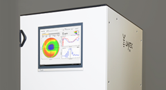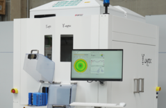
EpiX Mapping stations combine an XY-mapping stage with LayTec UV-VIS-NIR spectroscopic reflectance and photoluminescence metrology systems for a comprehensive 2D analysis of optical wafer properties by non-contact measurements. Integrated software provides full automated data analysis, including detection of VCSEL optical parameters (cavity dip, stop-band position), single layer and multiple layer thickness fits, film composition and multiple-peak analysis. Moreover, customers benefit from sample’s statistics and pass/fail classification on wafer-level and die-level.
The basic design feature of EpiX mapping stations is modularity and customizability in hardware and software. This is key for customers regularly adjusting their research projects to new materials and latest nano-science concepts. Hence EpiX is designed as a long-lasting workhorse with multiple upgrade options: more optical heads (wafer bow, reflectance-anisotropy, sheet-resistance, wafer thickness, optical transmission), extended wavelength range, software interfaces (e.g. for user-owned spectral analysis libraries) and for using in-situ data measured during epitaxy in center of wafer as starting point for post-epi 2D mapping analysis.

The latest configuration of EpiX also features a full cassette-to-cassette (C2C) wafer transport modification for high-throughput measurements in production environments. With this C2C option, LayTec now provides mapping solutions at the highest level of precision for both academic and industrial applications.
Downloads
Talk: UV-vis reflectance mapping of nitride-based device structures
Astrum LT chooses LayTec’s mapper for VCSEL manufacturing
EW MOVPE Ex-situ metrology for VCSEL epitaxy
Now available on YouTube
LayTec's EpiX Animation: Follow an epi-wafer on its path through the EpiX station
Dr. Johannes Zettler's talk on 'Connected metrology' at the Malvern Panalytical Future Days event

