 Epitaxial growth of UV LEDs faces significant challenges: long runs, superlattices, high Al content vs. high doping level, very high growth temperature large wafer bow and many more. LayTec's latest generation of EpiTT and EpiCurve®TT offers significant technology advances to solve most of these problems. Here are some application examples.
In-situ monitoring of high temperature AlN templates for UV LEDs
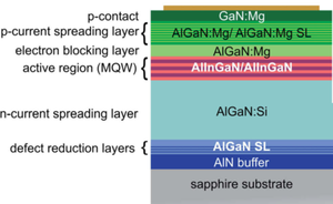
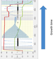
Fig. 1: State-of-the art UV-LED design according to “Chip designs for high efficiency III-nitride based ultraviolet light emitting diodes”, N. L. Ploch, PhD thesis, Technical University of Berlin 2015
Fig. 1 shows a layer stack of a typical UV LED structure to illustrate the growth steps monitored by LayTec's EpiTT and three in-situ parameters: temperature 405 nm reflectance and wafer bow as measured during two MOCVD of a typical UV LED structure. The data demonstrates, how precisely and accurately this combination of in-situ methods monitors the whole process.

Fig. 2: Two step MOCVD growth of UV-B LED (305 nm): 405 nm in-situ reflectance monitored by EpiTT. (HT=high temperature, LT=low temperature, NL=nucleation layer, SPSL=short-period superlattice)
In the course of LayTec's cooperation with FBH in the consortium "Advanced UV for Life", FBH scientists (Group of Prof. Markus Weyers) have developed a high temperature (HT) MOCVD process for growing low-defect-density AlN/sapphire templates for UV LEDs. The split of the UV LED growth in two separate steps in two different MOCVD systems fully avoids the possible memory effect related interference of AlGaN processes with the growth of high quality AlN buffers. The AlN buffer growth (Fig. 3) was monitored by 3 wavelength reflectance improved for very thick AlN/AlGaN layer stacks and by the emissivity corrected high temperature sensing of EpiTT Gen3. The blue curve is the result of the quantitative analysis of the 3 wavelength reflectance measured by EpiTT Gen3.

Fig. 3: In-situ reflectance at 405 nm, 633 nm and 950 nm of the two step growth of an AlN template structure for UV LEDs monitored: Blue curves - measured data, red curves - fitted data.
The thickness of the AlN nucleation layer is determined from the fitting curves (red) to be 43.2±0.2 nm, and the AlN high temperature buffer layer thickness to be 524.2±0.5 nm. The consistency of the used high temperature nk database is also obvious from the good agreement of the simulated curve segments in the temperature up-ramping and down-cooling steps.
The key for the unrivaled EpiTT Gen3 high temperature performance is not just the widened temperature sensing range, but, which is more important, also the high temperature nk database (up to 1500°C) for the AlN and AlGaN class of materials and improved performance for double-side polished sapphire wafers.
Alongside with temperature and reflectance, in-situ wafer bow monitoring is a further pathway to process and reactor optimization. Fig. 4 reveals the intrinsic challenge of AlN buffers for UV-LED yield: the wafer bow at the growth temperature of active region (TMQW) is always large, which finally leads to non-uniform UV-LED emission wavelength and, as a result, to lower yields.
Fig. 4: In-situ wafer bow measurements during growth of UV LED structure.
One of the methods to reduce the strain and annihilate dislocations is a short-period superlattice (SPSL) of GaN/AlN. Internal GaN/AlN interfaces are key for reducing dislocation density. In-situ reflectance at 405 nm in Fig. 5 directly shows the formation of these 160 interfaces between the ~1nm thick GaN/AlN layers. Ex-situ measurements in Fig. 6 confirm this.

Fig. 5: 405 nm reflectance measured in-situ (above) and simulated (below). The loupe shows the formation of GaN/AlN interfaces of SPSL.

Fig. 6: Ex-situ data: transition from AlN buffer to GaN/AlN superlattice. Red - Al, green - Ga, blue - N.
These examples prove that state-of-the art in-situ metrology is a must for process development and control of such complex devices as UV LEDs. For more information please contact info@laytec.de.
280 nm反射传感的氮化铝镓表面形态
铝含量高的氮化铝镓缓冲层是使UV-C LED达到最佳性能的必要条件。但其频段边界低于300nm,因此原有的405nm原位反射对该类氮化铝镓缓冲层的表面形态并不敏感。为在UV-C LED外延过程中精确监测氮化铝镓的生长速率和表面形态,LayTec提供了280nm的附加反射渠道,将UV-C LED作为光源。
图1为氮化铝镓层生长过程中的原位测量结果:由于材料的频段边界在生长温度下转向较长波长,因此氮化铝镓最终层的法布里-珀罗振荡渐次减弱。12000秒时反射率的小幅降低表明氮化铝镓表面略微粗糙。绿色的线表示高分辨率的翘曲度数据(参见下文)。本研究由 Advanced UV for Life公司提供资金支持.

图1:在Aixtron CCS 6x2反应器中,氮化铝/氮化铝镓(铝含量为60%)在蓝宝石/氮化铝模板上的生长情况:黑色—反射率280nm;蓝色—反射率405nm;绿色—高分辨率翘曲度;红色—实际温度。
紫外线LED: 使图形化蓝宝石衬底(pss)和双面抛光蓝宝石(dsp)获得准确温度值
对紫外线LED来说,辐射光通常通过蓝宝石衬底退出器件结构。因此,经常使用双面抛光(dsp)蓝宝石。另外,蓝宝石衬底的正面可以通过纳米图形化蓝宝石衬底(pss)改性,以增强光提取效率。两类衬底特性在外延生长过程中通常会形成不被认可的状况。比如,图1所示为具有不同温度梯度的状况。


图1:温度梯度的形成。950纳米的真实温度: 蓝色组件W5(ssp)/ 橙色组件W6(dsp)/黑色组件W8(pss)
a)通过传统发射率修正的红外高温计测量
b)通过EpiTT Gen3测量,消除了发射率效应和晶片背部和/或图形化蓝宝石衬底的杂散光/折光效应。
在不同基座组件中,晶片具有不同类型的蓝宝石衬底:dsp(双面抛光蓝宝石),pss(图形化蓝宝石衬底)和ssp(单面抛光蓝宝石衬底)。对于这些晶片类型,传统红外高温测定法(如图1a)可测量三种不同组件温度。Dsp(双面抛光蓝宝石)在900摄氏度时产生修正值,pss(图形化蓝宝石衬底)的温度为~10 K而ssp(单面抛光蓝宝石衬底)则比dsp(双面抛光蓝宝石)低~25 K。表观(而非真实)温度下降程度取决于温度、背面粗糙度、图形化蓝宝石衬底的图形和反应器配置。但是,EpiTT Gen3采用新的软件算法,考虑了上述特殊效应,对于ssp、dsp 和pss蓝宝石衬底都能产生同样准确的组件温度(图1b)。
克服紫外线LED外延中晶片和喷头之间的间距变化
对于紫外线LED工艺,EpiTT Gen3可测量高达1500摄氏度的温度。不过,全新的Gen3功能也非常重要:可选择两类测量探头:传统的光纤头(FOH)和全新的平行光束头(PBH)。
对于强耦合喷头(CCS)外延反应器来说,带平行光束头的测量工具是最佳选择,因为在这些反应器中晶片和喷头之间的间隔(距离)在一次外延生长过程中必须经过多次变化(调整),以便在紫外线LED流程中避免预反应,并形成较高生长率。
图3显示了偏离中心情况(图1a)下的光纤头(FOH)。
温度信号的“跃升”必须通过测量工具的多间隔校准来补偿。
同时,新的平行光束喷头(PBH)即便在间隔发生变化时(图1b)也能产生非常稳定的反射信号,无需在每次间隔变化时都进行间隔校准。


图1:间隔变化过程中的反射率(950纳米)和温度数据:
a) 光纤头(FOH)显示了相对于每个开氏温差的约30%的反射率降,具体根据样品结构而定。
b) 平行光束喷头(PBH)能产生稳定的反射率和温度信号。在标准间距(11毫米)下,两种喷头都可测量相同反射率。(数据通过绝对热参数测定)
Advanced 405 nm reflectance analysis for AlN buffer optimization in UV LEDs
At our Metrology Workshop during ICNS 2015 in Beijing Prof. Dabing Li of Chinese Academy of Sciencies (CAS) reported about AlN buffer optimization for UV LED growth by means of the 405 nm reflectance. The screenshot in Fig. 1 below shows in-situ reflectance (405 nm) data measured by EpiTT during high temperature MOCVD growth of AlN buffers for UV LEDs. Different surface morphology modes (2D and 3D) show up:

Fig. 1: Transition from 3D island growth to 2D growth in the two-step growth of AlN
You can download the complete talk as a PDF file here
Further reading: X. Sun et.al.: In situ observation of two-step growth of AlN on sapphire using high-temperature metal–organic chemical vapour deposition, CrystEngComm, 2013,15, 6066-6073
In-situ benefits for UV LEDs
- Optimization of UV LED epitaxy
- Early detection of process deviations and wafer defects
- Higher yield
- Better uniformity
- Excellent device performance
Downloads
EMMOVPE 2019: 280 nm reflectometry – helpful tool for in-situ control of AlN-based MOVPE-growthApplication Note: In-situ metrology solutions for UV LED growth
In-situ news
- Characterization of 2D materials growth 2022
- Best practices from the field: How to enhance epitaxy process performance by in-situ data
- EpiCurve® TT: AlInN composition control for III-Nitride VCSELs
- Major laser supplier chooses EpiTT FaceT for yield improvement
- EpiTT: optimizing MBE growth of InP-based quantum cascade lasers
- Plenary Talk at EWMOVPE 2019: Metrology for UV-LEDs, VCSEL and Power electronics
- EWMOVPE 2019: In-situ metrology enabling MOCVD on InP based materials on III-V on Si/SiO2 substrates for silicon photonics
- EpiX – a modular wafer mapping station for compound semiconductor research
- EpiTT Band Edge – for MBE of InP based VCSEL devices
- GaAs based edge-emitting high-power IR lasers – yield ramp-up by EpiTT FaceT
- EpiTT VCSEL – shipments to leading VCSEL manufacturer
- In-situ metrology system shipped to GaN-on-SiC customer
- Optimizing quantum cascade laser (QCL) epitaxy with EpiCurve® TTpocket satellite configuration
- In-situ metrology for VCSEL epitaxy with additional spectral reflectance sensing
- UV-C LEDs: AlGaN surface morphology monitored by 280 nm reflectance
- AIXTRON qualifies LayTec EpiNet 2016 software
- IQE equips complete fab with LayTec tools for MOCVD process monitoring
- AbsoluT 400 for temperature calibration of Pyro 400 is on the market!
- In-situ power for RF and power electronics
- Advanced in-situ analysis for UV LEDs
Advanced UV for Life
LayTec is a partner of the consortium "Advanced UV for Life" funded by the German Federal Ministry of Education and Research within the program "Twenty20 - Partnership for Innovation" (grant number 03ZZ0105C).![]()
![]()
![]()